
Customized Everything to Meet Your Needs
10 Years Professional Manufacturer Experience for Silicon Carbide Products
产品中心
—— PRODUCT CENTER ——
‹
›
‹
›
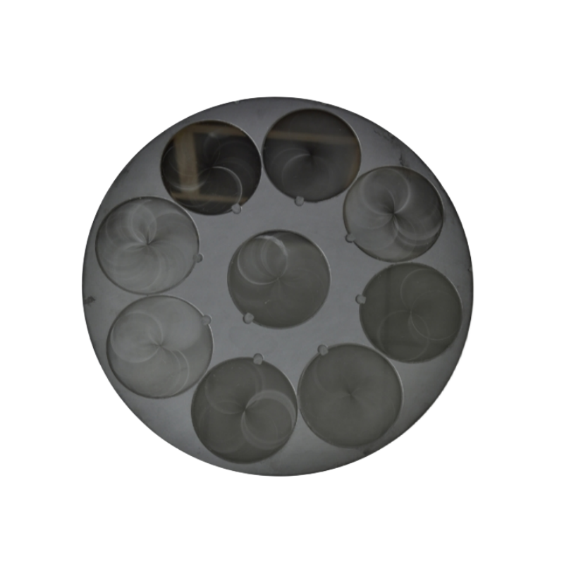
The silicon carbide ICP carrier is formed by isostatic pressing process and high-temperature sintering. According to the user's design drawings, the outer diameter, thickness, number and size of acupoints, as well as the position and shape of the tablet groove can also be precision processed to meet the specific usage requirements of the user.
Inductively Coupled Plasma (ICP) etching process applied in LED chip manufacturing, namely inductively coupled plasma etching.
Advantage:
1. Good thermal conductivity, low expansion coefficient, and average temperature performance
2. Resistance to plasma impact
3. It can be made according to the specific size requirements of the customer, with a maximum diameter of 495MM
4. Resistant to corrosion by various strong acids, strong alkalis, and chemical reagents
CONTACT US


